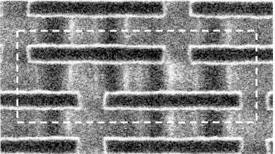
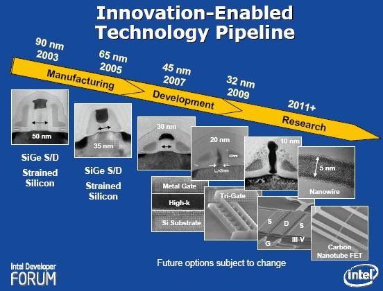
High-k dielectrics, metal gates and other novelties of the 45-nm process technology
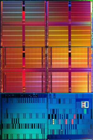
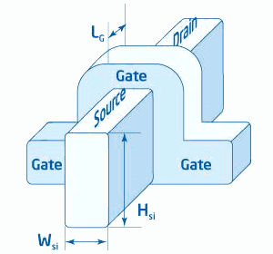
45 nm transistor
Introducing new process technologies, Intel is keeping pauses for about a year between the first demonstration of chips of new process technologies (normally, SRAM chips) and the demonstration of the first CPU specimens. That was the last time (65 nm) and this has happened again now.
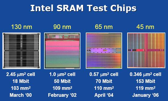
In a year after demonstration of the first 45-nm SRAM memory wafers, there have been demonstrated the first Penryn CPUs, with more details on the used materials and technologies provided. First of all, we should note that transition to new more precise process technologies entails the need for solving the issues of reducing the leakage currents in transistors, which directly affects the power consumption and heat emission of the chip in general, with all that being implemented under increased performance and complication of the CPU architecture and topology.
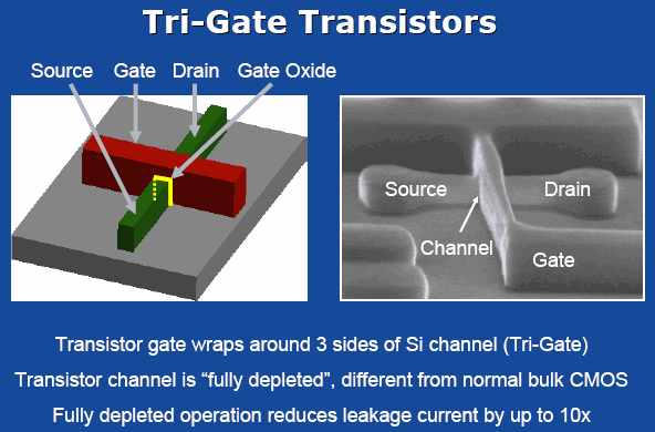
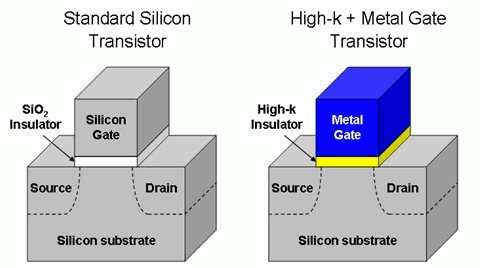
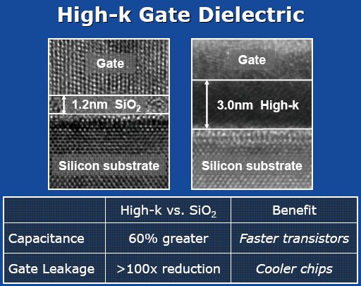
While moving to the 45-nm process technology to create transistor gates of low leakage currents, engineers at Intel had to use a new material for the dielectric - the so-called high-k dielectric combined with a new material of the transistor gate electrode made as a combination of metals. The thing is, the silicon dioxide (SiO2, traditionally used as the dielectric to create transistor gates for forty years, has simply run out of steam. In developing the previous 65-nm process technology, engineers at Intel succeeded in creation of a layer of dielectric made of silicon dioxide with alloy additions as thick as 1.2 nm – or as many as five atom layers!
However, further reduction in the thickness of the layer results in the direct tunneling effect and a sharp rise of leakage current through the material of the gate dielectric – in fact, silicon dioxide stops being an obstacle for a free electron drift which under these conditions demonstrate the properties of not only particles but waves, so there is no possibility of guaranteed control over the state of such a transistor.
A different type of dielectric helped solve this critical issue. To this end, silicon dioxide was replaced with a thin layer of material on the base of hafnium salts (rare-earth metals) having a high level of dielectric permeability k (high-k), which helped to reduce the leakage current by almost ten times as compared to the traditional silicon dioxide.
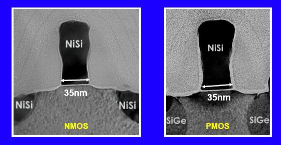
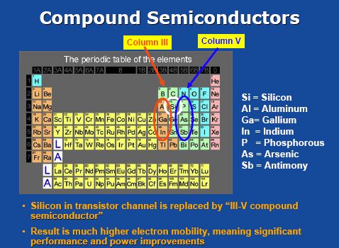
However, not all is as smooth as it looks. It's all right with physics, but chemistry of the new miraculous gate of high-k dielectric turned out to be incompatible to silicon traditionally used for the manufacture of gate electrodes, so the issue proved to be another nut to crack for Intel engineers when moving towards the 45-nm production process. There was a need to develop a new metal gate compatible to the new dielectric. Years were spent so as not only to find the suitable material for gate electrodes, but also to develop technologies of its use for gates of various conductivity - NMOS and PMOS.
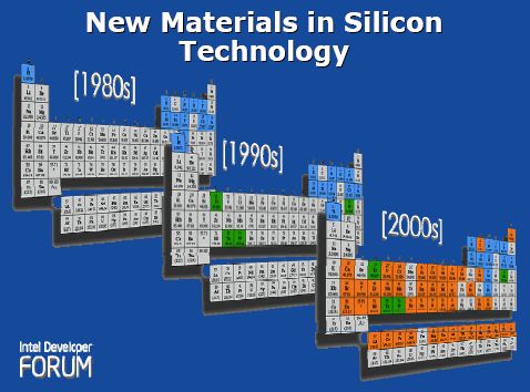
By the way, we should mention that the number of materials and chemical elements involved ion the production of modern chips is rising enormously. There used to be no more than ten to twenty quite recently, but now they count over half the Mendeleev periodic table!
Intel's 45-nm process technology is codenamed P1266, and the lithography used for the manufacture of Penryn is the same as that in the 65-nm process technology. Despite the new design of photo resists and new generation of photo masks, use of the same 193 nm lithographic tools allowed for substantial reduction of costs while moving to the 45-nm process technology.
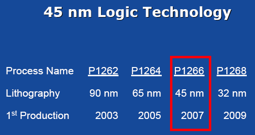
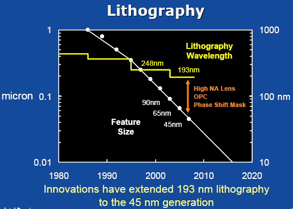
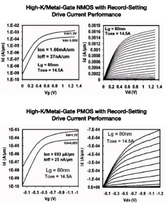
Intel's new 45-nm process technology implies smaller size of transistors with more dense positioning of these transistors on the wafer – almost twice as dense than in the previous 65 nm generation. The reduced dimensions of transistors have resulted in 30% drop of the current required for their switching, the switching speed of transistors has gone up by over 20%, and leakage currents in the "source-drain" channel have gone down by more than 5 times. Also, the leakage currents in the gate dielectric have dropped by over ten times. Some specialists call the introduction of high-k dielectrics and metal materials when creating the gate electrode a more complex and effective task than transition to a new precision process technology. It is also interesting to note that the next Intel's process technology P1268, 32-nm, is also quite likely to aim at using 193 nm lithographic tools.
Currently, Intel's new 45 process technology using 300 mm wafers is being introduced at Hillsborough, Oregon, at D1D factory. Among the most forthcoming plans of the company is the launch of 45-nm process at the new 300-mm Fab 32 in Ocotillo, Arizona (for mass production to be started in 2007) and Fab 28 in Israel (start of the mass production in the first half of 2008).
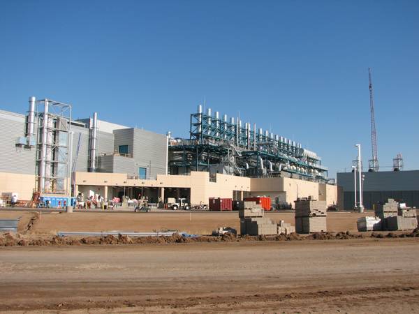
Fab 32 in Ocotillo, Arizona, under construction
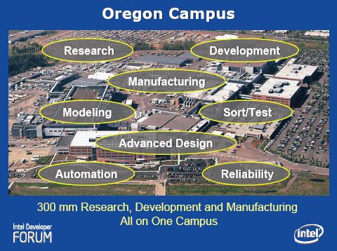
Intel's scientific research center in Hillsborough, Oregon, D1D
Practical implementation: Penryn in our motherboards
Despite the details of announcement, some details of the architecture and practical implementation of Penryn processors are not yet sufficient. For instance, we are in for telling about the new SSE4 instruction set which was first announced at the Fall IDF 2006.
For now it is still not clear which FSB speeds will be supported by the new processors, what clock speeds, and what motherboards will support them. There is information that the Penryn family of chips for desktop PCs will be originally presented in the familiar Socket 775, so it is quite possible that to make use of the existing motherboards it would suffice to update the BIOS, however, this info is still to be verified.
Lastly, closer to the mid-2007 Intel is about to plan presentation of new platforms with support for the new-generation DDR3 memory, and of course Penryn processors in these platforms are to play the first fiddle. I am absolutely sure that in the most immediate future we are going to know more and more details of the new design of Penryn processors once more and more briefings by Intel are held, and it is quite probable that the major "stratum" is still to be announced during the forthcoming IDFs in Taipei and Beijing.
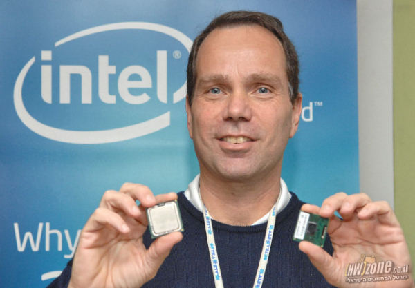
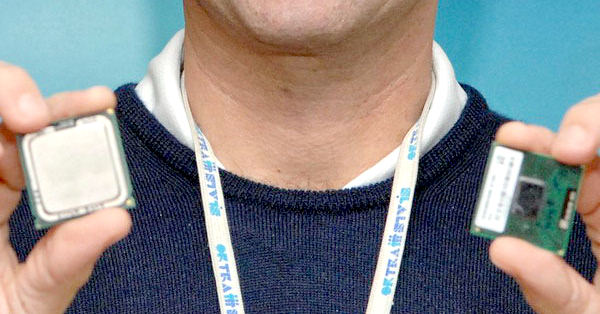
For today, that is about all the info on new processors, so we only bring in a photo of Penryn chips taken in the premises of Fab28 in Kiryat Gat, Israel, currently under construction (follow the link to an article in Hebrew. You are unlikely to read much without knowledge of the language but at the end of the page there is a comical movie on the construction of the factory). For today, we are closing the topic of Penryn chips and promise to come back to it once more details appear.
No comments:
Post a Comment