For the first time in the history of semiconductor industry, Intel today has officially introduced processors made following the 45-nm process technology. Merely a year has passed since Intel's demonstration of the first engineering samples of 45-nm SRAM memory, and now we see a new milestone to come: processors of the working name Penryn which comprise hundreds of millions of transistor gates made following the complex and "delicate" 45-nm process technology where the width of each transistor gate is as little as 35 nm.
Following the tradition, the announcement of CPU prototypes means that the production lines are in theory ready for wholesale manufacture - what is left is only a few verification arrangements and polishing of the equipment to the optimum chip yield. Afterwards, later to the summer a production of next-generation multicore Intel Core 2 Duo, Intel Core 2 Quad and Xeon processors will start, and their mass deliveries are planned for the second half of 2007.
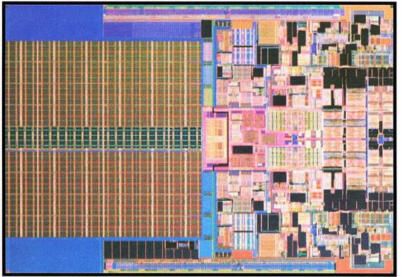
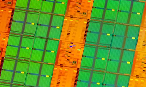
Photo of 45-nm CPU Intel Penryn
Intel's roadmap of CPU micro architectures and CPU designs
Today's even should be viewed from all the sides at a time due to a number of reasons. First, the 45-nm process technology was used in practice for the release of so complicated products. There have been of course serious modifications to the production technology as well as entirely new tools and materials at almost all the stages.
Secondly, transition to the so highly precise process technology with the evident change in physical and chemical properties of the circuit components called for use of absolutely new materials and technologies to handle the substrates, creation of transistor junctions, their electrodes etc. – whatever to attain lower leakage currents and more economical operation of the chip without the drop of performance per watt of energy spent.
Thirdly, the Penryn architecture of the CPU core has changed although they still are representatives of the Core (Merom) micro architecture. To avoid the mess of terms, we should recall that generations of CPU micro architectures change one another less frequently than various designs of cores (and even less frequently than new process technologies). For example, the NetBurst micro architecture which in 2000 came to replace the P6 micro architecture (the latest representatives of P6 are 0.18 mk Coppermine and the final 0.13 nm Tualatin in 2001) was in different times represented by a number of different core designs: Willamette (2000, 0.18 mk, 0.13 mk), Northwood (2002, 0.13 mk), Prescott/Smithfield (2004, 90 nm) and Cedar Mill/Presler (2006, 65 nm) – four generations of core design and six years on the same micro architecture!
At the same time, the Banias micro architecture presented in 2003 and which was progressing in parallel also contained a few generations of core architecture generations – Banias (2003, 0.13 mk), Dothan (2004, 90 nm), and Yonah (2006, 65 nm).
In fact, the emergence of new CPU core designs can be regarded as a gradual process of improvement within the same micro architecture with the addition of new features, redesign and scaling to a new process technology. At the same time, it turns out that Intel, due to two master scientific research centers working at the processor development – in Oregon and Israel, is developing and improving at least two micro architectures in parallel thus making use of the best practices of colleagues and getting rid of repeated errors.
The modern Core architecture which came in 2006 to replace the NetBurst and Banias, along with absolutely new engineering ideas and technologies, has inherited the best of the predecessors' experience. As a result, the very first design of the core having the working name Merom (2006, 65 nm) based on the Core micro architecture proved really successful in terms of performance and efficiency.
Today's novelty, the design of core of the working name Penryn is nothing more than the improved design of Merom with a simultaneous transition to the 45-nm process technology. The family of 45-nm Penryn chips will be the framework for new Core dual-core Wolfdale chips and 4-core Yorkfield chips which come to replace today's 65-nm Core 2 Duo and Core 2 Quad, respectively. Therefore, the processors of Penryn family will underlie the new generation of the mobile platform Intel Centrino codenamed Montevina. The new mobile platform Montevina which is expected in the first half of 2008 will replace the Santa Rosa version.
To sort out with the micro architectures of Intel processors and CPU core designs released on their base, let's look into the future. It is expected that the newly presented design of Penryn along with the Core micro architecture will survive for quite a long time – perhaps until 2010, and it is quite possible the processors with the Penryn core will be produced following the next, 32-nm, process technology.
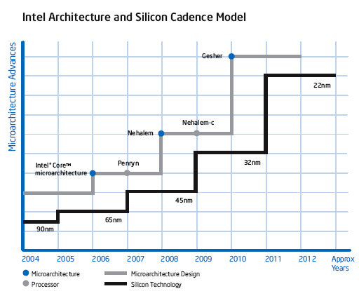
For now, we are not talking about the new versions of core designs based on the Core micro architecture, since next year (2008) we expect the announcement of an entirely new micro architecture of Intel's processors – Nehalem, based on which 45-nm processors of the same name Nehalem will be released closer to year 2009 , as well as Nehalem-C chips of the modified design. Further forecasts are still vague, but if everything goes as planned, then by 2010 we will see the first prototypes of chips built on the absolutely new micro architecture Gesher, and we only have to guess which process technology – 32 nm or 25 nm - will be used.
Penryn CPU architectural specifics
Anyway, let's come back to Penryn processors based on the Core micro architecture: according to the official statement of Intel's representatives, the company is currently offering five products of earlier steppings aimed at various sectors of the market- over 15 chips planned for the forthcoming release following the 45-nm process technology. According to the company's statements, Penryn chips are already under trial runs in systems powered by Windows Vista, Mac OS X, Windows XP, and Linux.
As per the practical experience (or maybe the tradition?) acquired during the release of first chips of the Core micro architecture, the Penryn family will include desktop and mobile PCs, workstations and corporate systems.
We'll be considering the technology changes that touched upon the manufacturing process and materials used later, but for now let's list the innovations implemented in the Penryn processors. Among them is the increased number of transistors – over 410 mln for the dual-core design (291 mln transistors in 65-nm dual-core Conroe) and over 820 mln for the quad-core Yorkfield, with the chip area reduced to 110 mm2 (from 143 mm2 in Conroe). That's where we see preservation of the Moore's Law according to which the quantity of transistors is doubled once every two years, with the unit cost of manufacture per single transistor going down and the performance going up, and in the near future - I am sure - we can ascertain the doubling of CPU cores on a chip, why not?
Along with that, the Penryn family of CPUs will support for up to 50 new Intel SSE4 instructions aimed at the increase of capabilities and performance of handling the multimedia content. In this regard, it is interesting to note that support for a number of new SSE instructions was announced still for Conroe processors, however at IDF Fall 2006 the support for SSE4 was reserved for the next generation of micro architecture, Nehalem. As is stated in the press release, Penryn will support for the new Intel SSE4 instruction set.
Among the new chips there will be versions of L2 cache size up to 12 MB, and in general the whole family will differ in increased performance and advanced capabilities of controlling the power consumption modes. As to the power consumption of new 45-nm Core 2 Duo, Core 2 Extreme, Core 2 Quad, and Xeon processors based on the Penryn core, it is already known that the TDP will be approximately matching to today's realities – about 35 W in chips for notebooks, about 65 W in the mainstream chips for desktop PCs, about 80 W in 4-core server processors and chips for extreme gamers, under increased performance.
No comments:
Post a Comment